Document Outline
- Main Directory
- ispLSI and pLSI 1032E Data Sheet
- DC Electrical Characteristics
- AC Characteristics
- Pin Configuration: 84-Pin PLCC
- Pin Configuration: 100-Pin TQFP
- Ordering Information
1
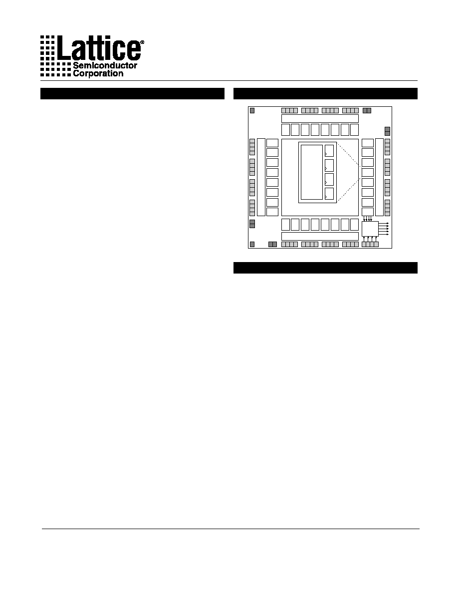
Functional Block Diagram
Features
∑ HIGH DENSITY PROGRAMMABLE LOGIC
-- 6000 PLD Gates
-- 64 I/O Pins, Eight Dedicated Inputs
-- 192 Registers
-- High Speed Global Interconnect
-- Wide Input Gating for Fast Counters, State
Machines, Address Decoders, etc.
-- Small Logic Block Size for Random Logic
∑ HIGH PERFORMANCE E
2
CMOS
Æ
TECHNOLOGY
--
f
max = 125 MHz Maximum Operating Frequency
--
t
pd = 7.5 ns Propagation Delay
-- TTL Compatible Inputs and Outputs
-- Electrically Erasable and Reprogrammable
-- Non-Volatile
-- 100% Tested at Time of Manufacture
-- Unused Product Term Shutdown Saves Power
∑ ispLSI OFFERS THE FOLLOWING ADDED FEATURES
-- In-System Programmable (ISPTM) 5-Volt Only
-- Increased Manufacturing Yields, Reduced Time-to-
Market and Improved Product Quality
-- Reprogram Soldered Devices for Faster Prototyping
∑ OFFERS THE EASE OF USE AND FAST SYSTEM
SPEED OF PLDs WITH THE DENSITY AND FLEXIBILITY
OF FIELD PROGRAMMABLE GATE ARRAYS
-- Complete Programmable Device Can Combine Glue
Logic and Structured Designs
-- Enhanced Pin Locking Capability
-- Four Dedicated Clock Input Pins
-- Synchronous and Asynchronous Clocks
-- Programmable Output Slew Rate Control to
Minimize Switching Noise
-- Flexible Pin Placement
-- Optimized Global Routing Pool Provides Global
Interconnectivity
∑ ispLSI DEVELOPMENT TOOLS
ispVHDLTM Systems
-- VHDL/Verilog-HDL/Schematic Design Options
-- Functional/Timing/VHDL Simulation Options
ispDSTM Software
-- Lattice HDL or Boolean Logic Entry
-- Functional Simulator and Waveform Viewer
ispDS+TM HDL Synthesis-Optimized Logic Fitter
-- Supports Leading Third-Party Design Environments
for Schematic Capture, Synthesis and Timing
Simulation
-- Static Timing Analyzer
ISP Daisy Chain Download Software
Output Routing Pool
Output Routing Pool
D7 D6 D5 D4 D3 D2 D1 D0
B0 B1 B2 B3 B4 B5 B6 B7
A0
A1
A2
A3
A4
A5
A6
A7
C7
C6
C5
C4
C3
C2
C1
C0
Output Routing Pool
Output Routing Pool
CLK
Global Routing Pool (GRP)
0139A(A1)-isp
Logic
Array
D Q
D Q
D Q
D Q
GLB
Description
The ispLSI and pLSI 1032E are High Density Program-
mable Logic Devices containing 192 Registers, 64
Universal I/O pins, eight Dedicated Input pins, four Dedi-
cated Clock Input pins and a Global Routing Pool (GRP).
The GRP provides complete interconnectivity between
all of these elements. The ispLSI 1032E features 5-Volt
in-system programmability and in-system diagnostic ca-
pabilities. The ispLSI 1032E device offers non-volatile
reprogrammability of the logic, as well as the intercon-
nects to provide truly reconfigurable systems. It is
architecturally and parametrically compatible to the pLSI
1032E device, but multiplexes four input pins to control
in-system programming. A functional superset of the
ispLSI and pLSI 1032 architecture, the ispLSI and pLSI
1032E devices add two new global output enable pins.
The basic unit of logic on the ispLSI and pLSI 1032E
devices is the Generic Logic Block (GLB). The GLBs are
labeled A0, A1...D7 (see Figure 1). There are a total of 32
GLBs in the ispLSI and pLSI 1032E devices. Each GLB
has 18 inputs, a programmable AND/OR/Exclusive OR
array, and four outputs which can be configured to be
either combinatorial or registered. Inputs to the GLB
come from the GRP and dedicated inputs. All of the GLB
outputs are brought back into the GRP so that they can
be connected to the inputs of any GLB on the device.
ispLSI
Æ
and pLSI
Æ
1032E
High-Density Programmable Logic
1032E_05
Copyright © 1997 Lattice Semiconductor Corp. All brand or product names are trademarks or registered trademarks of their respective holders. The specifications and information herein are subject
to change without notice.
LATTICE SEMICONDUCTOR CORP., 5555 Northeast Moore Ct., Hillsboro, Oregon 97124, U.S.A.
July 1997
Tel. (503) 681-0118; 1-800-LATTICE; FAX (503) 681-3037; http://www.latticesemi.com
2
Specifications
ispLSI and pLSI 1032E
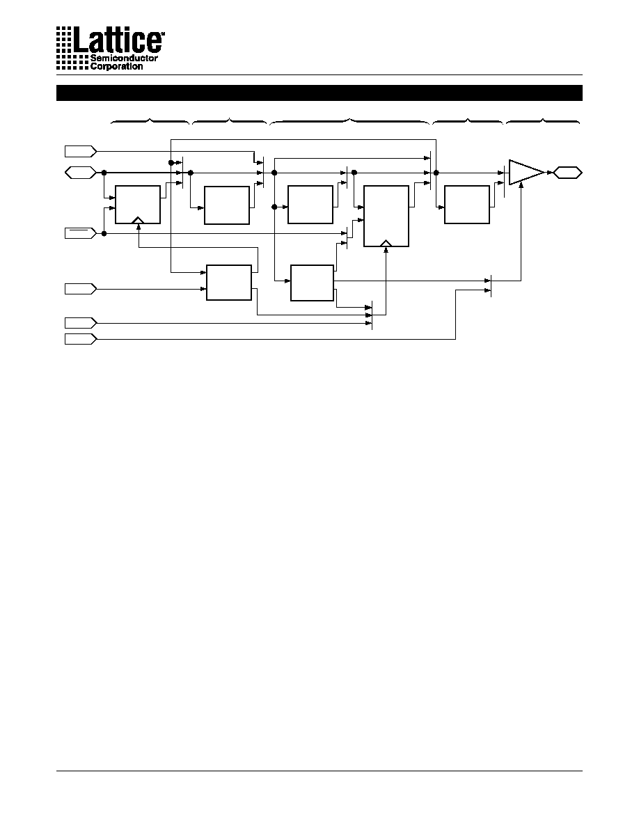
Functional Block Diagram
Figure 1. ispLSI and pLSI 1032E Functional Block Diagram
The devices also have 64 I/O cells, each of which is
directly connected to an I/O pin. Each I/O cell can be
individually programmed to be a combinatorial input,
registered input, latched input, output or bi-directional
I/O pin with 3-state control. The signal levels are TTL
compatible voltages and the output drivers can source 4
mA or sink 8 mA. Each output can be programmed
independently for fast or slow output slew rate to mini-
mize overall output switching noise.
Eight GLBs, 16 I/O cells, two dedicated inputs and one
ORP are connected together to make a Megablock (see
figure 1). The outputs of the eight GLBs are connected to
a set of 16 universal I/O cells by the ORP. Each ispLSI
and pLSI 1032E device contains four Megablocks.
The GRP has, as its inputs, the outputs from all of the
GLBs and all of the inputs from the bi-directional I/O cells.
All of these signals are made available to the inputs of the
GLBs. Delays through the GRP have been equalized to
minimize timing skew.
Clocks in the ispLSI and pLSI 1032E devices are se-
lected using the Clock Distribution Network. Four
dedicated clock pins (Y0, Y1, Y2 and Y3) are brought into
the distribution network, and five clock outputs (CLK 0,
CLK 1, CLK 2, IOCLK 0 and IOCLK 1) are provided to
route clocks to the GLBs and I/O cells. The Clock Distri-
bution Network can also be driven from a special clock
GLB (C0 on the ispLSI and pLSI 1032E devices). The
logic of this GLB allows the user to create an internal
clock from a combination of internal signals within the
device.
I/O 63
I/O 62
I/O 61
I/O 60
RESET
Global
Routing
Pool
(GRP)
CLK 0
CLK 1
CLK 2
IOCLK 0
IOCLK 1
Clock
Distribution
Network
C7
C6
C5
C4
C3
C2
C1
C0
A7
A6
A5
A4
A3
A2
A1
A0
Generic
Logic Blocks
(GLBs)
Megablock
Output Routing Pool (ORP)
Output Routing Pool (ORP)
Output Routing Pool (ORP)
Output Routing Pool (ORP)
Input Bus
Input Bus
*ispEN/NC
lnput Bus
lnput Bus
*ISP Control Functions for ispLSI 1032E Only
I/O 59
I/O 58
I/O 57
I/O 56
I/O 55
I/O 54
I/O 53
I/O 52
I/O 51
I/O 50
I/O 49
I/O 48
IN 7
IN 6
D7
D6
D5
D4
D3
D2
D1
D0
I/O 16
I/O 17
I/O 18
I/O 19
*SDO/IN 2
*SCLK/IN 3
I/O 20
I/O 21
I/O 22
I/O 23
I/O 24
I/O 25
I/O 26
I/O 27
I/O 28
I/O 29
I/O 30
I/O 31
I/O 35
I/O 34
I/O 33
I/O 32
I/O 0
I/O 1
I/O 2
I/O 3
I/O 12
I/O 13
I/O 14
I/O 15
*SDI/IN 0
*MODE/IN 1
I/O 8
I/O 9
I/O 10
I/O 11
I/O 4
I/O 5
I/O 6
I/O 7
I/O 47
I/O 46
I/O 45
I/O 44
GOE 1/IN 5
GOE 0/IN 4
I/O 43
I/O 42
I/O 41
I/O 40
I/O 39
I/O 38
I/O 37
I/O 36
Y0
Y1
Y2
Y3
B0
B1
B2
B3
B4
B5
B6
B7

3
Specifications
ispLSI and pLSI 1032E
Absolute Maximum Ratings
1
Supply Voltage V
cc
................................... -0.5 to +7.0V
Input Voltage Applied ........................ -2.5 to V
CC
+1.0V
Off-State Output Voltage Applied ..... -2.5 to V
CC
+1.0V
Storage Temperature ................................ -65 to 150
∞
C
Case Temp. with Power Applied .............. -55 to 125
∞
C
Max. Junction Temp. (T
J
) with Power Applied ... 150
∞
C
1. Stresses above those listed under the "Absolute Maximum Ratings" may cause permanent damage to the device. Functional
operation of the device at these or at any other conditions above those indicated in the operational sections of this specifica tion
is not implied (while programming, follow the programming specifications).
DC Recommended Operating Conditions
T
A
= 0
∞
C to + 70
∞
C
T
A
= -40
∞
C to + 85
∞
C
SYMBOL
Table 2-0005/1032E
V
CC
V
IH
V
IL
PARAMETER
Supply Voltage
Input High Voltage
Input Low Voltage
MIN.
MAX.
UNITS
4.75
4.5
2.0
0
5.25
5.5
V
cc
+1
0.8
V
V
V
V
Commercial
Industrial
Capacitance (T
A
=25
o
C, f=1.0 MHz)
Data Retention Specifications
Table 2-0008/1032E
PARAMETER
pLSI Erase/Reprogram Cycles
100
Data Retention
MINIMUM
MAXIMUM
UNITS
ispLSI Erase/Reprogram Cycles
20
10000
≠
≠
≠
Cycles
Years
Cycles
C
SYMBOL
Table 2-0006/1032E
C
PARAMETER
Y0 Clock Capacitance
15
UNITS
TYPICAL
TEST CONDITIONS
1
2
8
Dedicated Input, I/O, Y1, Y2, Y3, Clock Capacitance
(Commercial/Industrial)
pf
pf
V = 5.0V, V = 2.0V
V = 5.0V, V = 2.0V
CC
CC
PIN
PIN
4
Specifications
ispLSI and pLSI 1032E
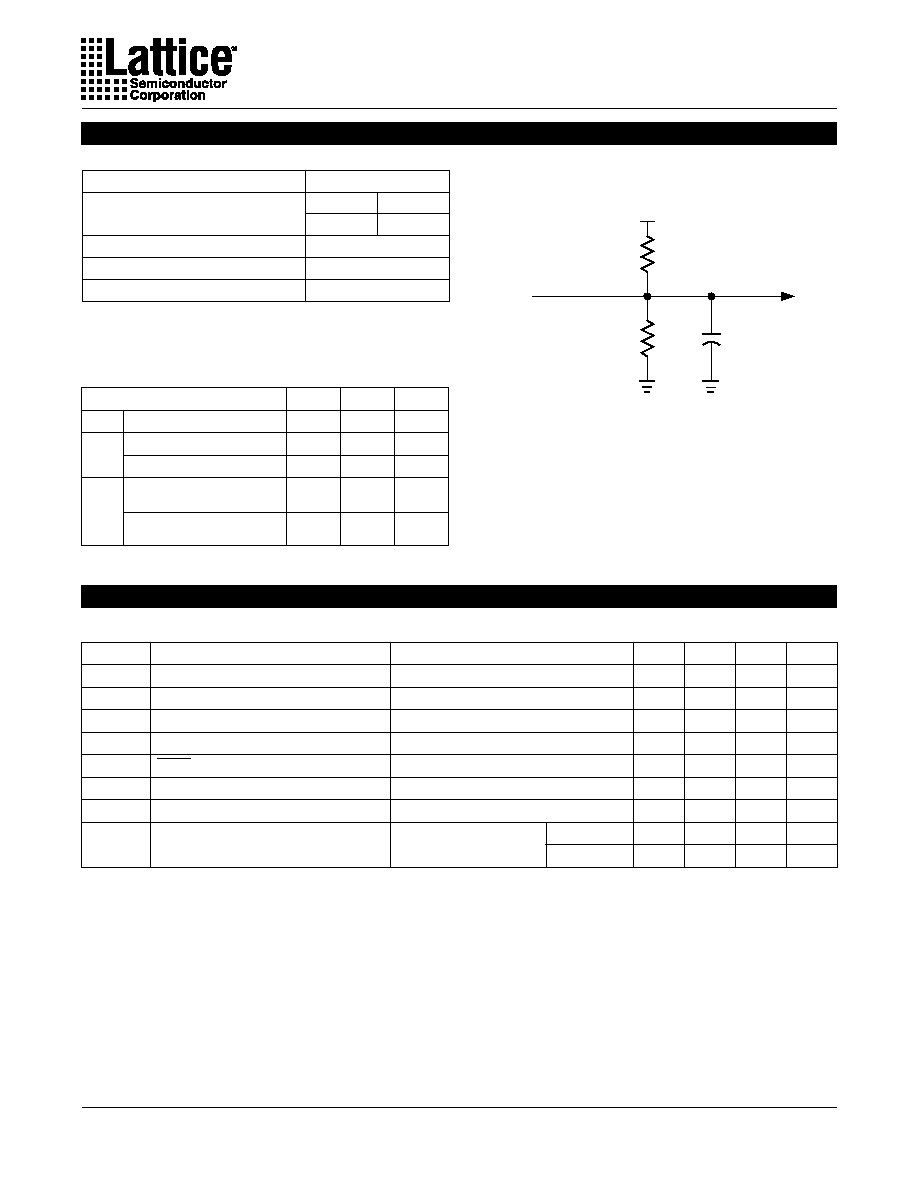
Output Load Conditions (see Figure 2)
Switching Test Conditions
TEST CONDITION
R1
R2
CL
A
470
390
35pF
B
390
35pF
470
390
35pF
Active High
Active Low
C
470
390
5pF
390
5pF
Active Low to Z
at V +0.5V
OL
Active High to Z
at V -0.5V
OH
Table 2-0004/1032E
Figure 2. Test Load
+ 5V
R1
R2
CL
*
Device
Output
Test
Point
*
CL includes Test Fixture and Probe Capacitance.
0213a
DC Electrical Characteristics
Over Recommended Operating Conditions
V
OL
SYMBOL
1. One output at a time for a maximum duration of one second. V = 0.5V was selected to avoid test problems
by tester ground degradation. Characterized but not 100% tested.
2. Measured using eight 16-bit counters.
3. Typical values are at V = 5V and T = 25
∞
C.
4. Maximum I varies widely with specific device configuration and operating frequency. Refer to the Power Consumption
section of this data sheet and Thermal Management section of the Lattice Semiconductor Data Book or CD-ROM to
estimate maximum I .
Table 2-0007/1032E
1
V
OH
I
IH
I
IL
I
IL-isp
PARAMETER
I
IL-PU
I
OS
2, 4
I
CC
Output Low Voltage
Output High Voltage
Input or I/O High Leakage Current
Input or I/O Low Leakage Current
ispEN Input Low Leakage Current
I/O Active Pull-Up Current
Output Short Circuit Current
Operating Power Supply Current
I = 8 mA
I = -4 mA
3.5V
V
V
0V
V
V (Max.)
0V
V
V
0V
V
V
V = 5V, V = 0.5V
V = 0.5V, V = 3.0V
f = 1 MHz
OL
OH
IN IL
IN CC
IN
IL
IN IL
CC OUT
CLOCK
IL
IH
CONDITION
MIN.
TYP.
MAX.
UNITS
3
≠
2.4
≠
≠
≠
≠
≠
≠
≠
≠
≠
≠
≠
≠
≠
≠
190
190
0.4
≠
10
-10
-150
-150
-200
≠
≠
V
V
µ
A
µ
A
µ
A
µ
A
mA
mA
mA
CC
A
OUT
CC
CC
Commercial
Industrial
Input Pulse Levels
Table 2-0003/1032E
Input Rise and Fall Time
10% to 90%
Input Timing Reference Levels
Ouput Timing Reference Levels
Output Load
GND to 3.0V
1.5V
1.5V
See Figure 2
3-state levels are measured 0.5V from
steady-state active level.
-125
Others
2 ns
3 ns

5
Specifications
ispLSI and pLSI 1032E
t
pd1
UNITS
TEST
COND.
1. Unless noted otherwise, all parameters use the GRP, 20 PTXOR path, ORP and Y0 clock.
2. Refer to Timing Model
in this data sheet for further details.
3. Standard 16-bit counter using GRP feedback.
4. Reference Switching Test Conditions section.
Table 2-0030A/1032E
1
4
3
1
tsu2 + tco1
( )
-100
MIN. MAX.
DESCRIPTION
#
2
PARAMETER
A
1
Data Propagation Delay, 4PT Bypass, ORP Bypass
≠
10.0
ns
t
pd2
A
2
Data Propagation Delay, Worst Case Path
≠
ns
f
max (Int.)
A
3
Clock Frequency with Internal Feedback
100
≠
MHz
f
max (Ext.)
≠
4
Clock Frequency with External Feedback
≠
MHz
f
max (Tog.)
≠
5
Clock Frequency, Max. Toggle
≠
MHz
t
su1
≠
6
GLB Reg. Setup Time before Clock,4 PT Bypass
≠
ns
t
co1
A
7
GLB Reg. Clock to Output Delay, ORP Bypass
≠
ns
t
h1
≠
8
GLB Reg. Hold Time after Clock, 4 PT Bypass
≠
ns
t
su2
≠
9
GLB Reg. Setup Time before Clock
≠
ns
t
co2
≠
10
GLB Reg. Clock to Output Delay
≠
ns
t
h2
≠
11
GLB Reg. Hold Time after Clock
≠
ns
t
r1
A
12
Ext. Reset Pin to Output Delay
≠
ns
t
rw1
≠
13
Ext. Reset Pulse Duration
≠
ns
t
ptoeen
B
14
Input to Output Enable
≠
ns
t
ptoedis
C
15
Input to Output Disable
≠
ns
t
wh
≠
18
External Synchronous Clock Pulse Duration, High
4.0
ns
t
wl
≠
19
External Synchronous Clock Pulse Duration, Low
4.0
ns
t
su3
≠
20
I/O Reg. Setup Time before Ext. Sync Clock (Y2, Y3)
≠
ns
t
h3
≠
21
I/O Reg. Hold Time after Ext. Sync. Clock (Y2, Y3)
≠
ns
71.0
125
7.0
0.0
8.0
0.0
6.5
3.5
0.0
12.5
6.0
7.0
13.5
15.0
15.0
≠
≠
( )
1
twh + tw1
t
goeen
B
16
Global OE Output Enable
≠
ns
9.0
t
goedis
C
17
Global OE Output Disable
≠
ns
9.0
-125
MIN. MAX.
≠
7.5
≠
125
≠
≠
≠
≠
≠
≠
≠
≠
≠
≠
≠
≠
≠
3.0
3.0
≠
≠
91.0
167
5.0
0.0
6.0
0.0
5.0
3.0
0.0
10.0
5.0
6.0
10.0
12.0
12.0
≠
≠
≠
7.0
≠
7.0
External Timing Parameters
Over Recommended Operating Conditions
6
Specifications
ispLSI and pLSI 1032E
USE 1032E-100 FOR
NEW DESIGNS
t
pd1
UNITS
TEST
COND.
1. Unless noted otherwise, all parameters use the GRP, 20 PTXOR path, ORP and Y0 clock.
2. Refer to Timing Model
in this data sheet for further details.
3. Standard 16-bit counter using GRP feedback.
4. Reference Switching Test Conditions section.
Table 2-0030B/1032E
1
4
3
1
tsu2 + tco1
( )
-70
MIN. MAX.
DESCRIPTION
#
2
PARAMETER
A
1
Data Propagation Delay, 4PT Bypass, ORP Bypass
≠
15.0
ns
t
pd2
A
2
Data Propagation Delay, Worst Case Path
≠
ns
f
max (Int.)
A
3
Clock Frequency with Internal Feedback
70.0
≠
MHz
f
max (Ext.)
≠
4
Clock Frequency with External Feedback
≠
MHz
f
max (Tog.)
≠
5
Clock Frequency, Max. Toggle
≠
MHz
t
su1
≠
6
GLB Reg. Setup Time before Clock,4 PT Bypass
≠
ns
t
co1
A
7
GLB Reg. Clock to Output Delay, ORP Bypass
≠
ns
t
h1
≠
8
GLB Reg. Hold Time after Clock, 4 PT Bypass
≠
ns
t
su2
≠
9
GLB Reg. Setup Time before Clock
≠
ns
t
co2
≠
10
GLB Reg. Clock to Output Delay
≠
ns
t
h2
≠
11
GLB Reg. Hold Time after Clock
≠
ns
t
r1
A
12
Ext. Reset Pin to Output Delay
≠
ns
t
rw1
≠
13
Ext. Reset Pulse Duration
≠
ns
t
ptoeen
B
14
Input to Output Enable
≠
ns
t
ptoedis
C
15
Input to Output Disable
≠
ns
t
wh
≠
18
External Synchronous Clock Pulse Duration, High
5.0
ns
t
wl
≠
19
External Synchronous Clock Pulse Duration, Low
5.0
ns
t
su3
≠
20
I/O Reg. Setup Time before Ext. Sync Clock (Y2, Y3)
≠
ns
t
h3
≠
21
I/O Reg. Hold Time after Ext. Sync. Clock (Y2, Y3)
≠
ns
56.0
100
9.0
0.0
11.0
0.0
10.0
4.0
0.0
17.5
7.0
8.0
15.0
18.0
18.0
≠
≠
( )
1
twh + tw1
t
goeen
B
16
Global OE Output Enable
≠
ns
12.0
t
goedis
C
17
Global OE Output Disable
≠
ns
-90
MIN. MAX.
≠
10.0
≠
90.0
≠
≠
≠
≠
≠
0.0
8.5
≠
0.0
≠
6.5
≠
≠
4.0
4.0
3.5
≠
0.0
≠
69.0
125
7.5
6.0
≠
≠
7.0
≠
13.5
≠
15.0
15.0
≠
≠
12.5
≠
9.0
≠
9.0
12.0
-80
MIN. MAX.
≠
12.0
≠
80.0
≠
≠
≠
≠
≠
≠
≠
≠
≠
≠
≠
≠
≠
4.5
4.5
≠
≠
61.0
111
8.5
0.0
10.0
0.0
8.0
3.5
0.0
15.0
6.5
7.5
14.0
16.5
16.5
≠
≠
≠
10.0
≠
10.0
External Timing Parameters
Over Recommended Operating Conditions
7
Specifications
ispLSI and pLSI 1032E
GRP Delay, 32 GLB Loads
t
iobp
1. Internal Timing Parameters are not tested and are for reference only.
2. Refer to Timing Model in this data sheet for further details.
3. The XOR adjacent path can only be used by hard macros.
Table 2-0036A/1032E
Inputs
UNITS
-100
MIN.
MIN.
MAX.
MAX.
DESCRIPTION
#
2
PARAM.
22 I/O Register Bypass
ns
t
iolat
23 I/O Latch Delay
ns
t
grp32
33
ns
GLB
t
1ptxor
36 1 Prod.Term/XOR Path Delay
ns
t
20ptxor 37 20 Prod. Term/XOR Path Delay
ns
t
xoradj
38 XOR Adjacent Path Delay
ns
t
gbp
39 GLB Register Bypass Delay
ns
t
gsu
40 GLB Register Setup Time before Clock
ns
t
gh
41 GLB Register Hold Time after Clock
ns
t
gco
42 GLB Register Clock to Output Delay
ns
3
t
gro
43 GLB Register Reset to Output Delay
ns
t
ptre
44 GLB Prod.Term Reset to Register Delay
ns
t
ptoe
45 GLB Prod. Term Output Enable to I/O Cell Delay
ns
t
ptck
46 GLB Prod. Term Clock Delay
ns
ORP
GRP
t
4ptbpc
34 4 Prod.Term Bypass Path Delay (Combinatorial)
ns
t
4ptbpr
35 4 Prod. Term Bypass Path Delay (Registered)
ns
t
orp
47 ORP Delay
ns
t
orpbp
48 ORP Bypass Delay
ns
t
iosu
24 I/O Register Setup Time before Clock
ns
t
ioh
25 I/O Register Hold Time after Clock
ns
t
ioco
26 I/O Register Clock to Out Delay
ns
t
ior
27 I/O Register Reset to Out Delay
ns
t
din
28 Dedicated Input Delay
ns
t
grp16
32 GRP Delay, 16 GLB Loads
ns
t
grp8
31 GRP Delay, 8 GLB Loads
ns
t
grp4
30 GRP Delay, 4 GLB Loads
ns
t
grp1
29 GRP Delay, 1 GLB Load
ns
0.0
-125
≠
≠
≠
≠
≠
≠
≠
≠
≠
≠
≠
≠
≠
0.1
4.5
2.9
≠
≠
3.0
0.0
≠
≠
≠
≠
≠
≠
≠
0.3
1.9
3.8
3.6
5.0
5.0
0.4
2.3
4.9
3.9
5.4
3.9
4.0
≠
≠
4.0
1.0
0.0
≠
≠
4.6
4.6
2.3
2.8
2.3
2.0
1.8
≠
≠
≠
≠
≠
≠
≠
≠
≠
≠
≠
≠
≠
0.5
5.8
3.5
≠
≠
3.5
0.0
≠
≠
≠
≠
≠
≠
≠
0.3
2.3
4.2
4.6
5.8
6.3
1.0
2.5
6.2
4.5
7.2
5.3
5.3
≠
≠
4.7
1.0
≠
≠
5.0
5.0
2.7
3.0
2.4
2.4
1.9
Internal Timing Parameters
1

8
Specifications
ispLSI and pLSI 1032E
Internal Timing Parameters
1
USE 1032E-100 FOR
NEW DESIGNS
GRP Delay, 32 GLB Loads
t
iobp
1. Internal Timing Parameters are not tested and are for reference only.
2. Refer to Timing Model in this data sheet for further details.
3. The XOR adjacent path can only be used by hard macros.
Table 2-0036B/1032E
Inputs
UNITS
-80
MIN.
-70
MIN.
MAX.
MAX.
DESCRIPTION
#
2
PARAM.
22 I/O Register Bypass
≠
ns
t
iolat
23 I/O Latch Delay
≠
ns
t
grp32
33
≠
ns
GLB
t
1ptxor
36 1 Prod.Term/XOR Path Delay
≠
ns
t
20ptxor 37 20 Prod. Term/XOR Path Delay
≠
ns
t
xoradj
38 XOR Adjacent Path Delay
≠
ns
t
gbp
39 GLB Register Bypass Delay
≠
ns
t
gsu
40 GLB Register Setup Time before Clock
ns
t
gh
41 GLB Register Hold Time after Clock
ns
t
gco
42 GLB Register Clock to Output Delay
≠
ns
3
t
gro
43 GLB Register Reset to Output Delay
≠
ns
t
ptre
44 GLB Prod.Term Reset to Register Delay
≠
ns
t
ptoe
45 GLB Prod. Term Output Enable to I/O Cell Delay
≠
ns
t
ptck
46 GLB Prod. Term Clock Delay
ns
ORP
GRP
MIN. MAX.
t
4ptbpc
34 4 Prod.Term Bypass Path Delay (Combinatorial)
≠
ns
t
4ptbpr
35 4 Prod. Term Bypass Path Delay (Registered)
≠
ns
0.5
7.9
4.5
t
orp
47 ORP Delay
≠
ns
t
orpbp
48 ORP Bypass Delay
≠
0.0
ns
t
iosu
24 I/O Register Setup Time before Clock
3.5
ns
t
ioh
25 I/O Register Hold Time after Clock
0.0
ns
t
ioco
26 I/O Register Clock to Out Delay
≠
ns
t
ior
27 I/O Register Reset to Out Delay
≠
ns
t
din
28 Dedicated Input Delay
≠
ns
t
grp16
32 GRP Delay, 16 GLB Loads
≠
ns
t
grp8
31 GRP Delay, 8 GLB Loads
≠
ns
t
grp4
30 GRP Delay, 4 GLB Loads
≠
ns
t
grp1
29 GRP Delay, 1 GLB Load
≠
ns
0.3
2.7
4.8
6.6
7.8
8.2
1.3
2.9
6.4
5.5
8.0
7.1
6.7
≠
≠
5.8
1.0
0.0
≠
≠
5.4
5.4
2.8
3.5
2.8
2.5
2.2
≠
≠
≠
≠
≠
≠
≠
≠
≠
≠
≠
≠
≠
0.5
8.8
4.8
≠
≠
4.0
0.0
≠
≠
≠
≠
≠
≠
≠
0.3
3.3
5.6
8.3
8.7
9.2
1.6
2.9
6.8
5.8
9.0
8.8
7.2
≠
≠
6.2
1.0
≠
≠
6.1
6.0
2.8
4.0
3.2
2.5
2.5
-90
≠
≠
≠
≠
≠
≠
≠
≠
≠
≠
≠
≠
≠
≠
0.2
6.8
4.1
≠
3.5
0.0
≠
≠
≠
≠
≠
≠
≠
0.3
2.3
4.4
5.6
6.8
7.1
0.4
2.9
6.3
5.1
7.1
5.7
6.1
≠
≠
5.3
1.0
0.0
≠
≠
5.0
5.0
2.6
3.2
2.6
2.3
2.1

9
Specifications
ispLSI and pLSI 1032E
Internal Timing Parameters
1
t
ob
1. Internal Timing Parameters are not tested and are for reference only.
Table 2-0037A/1032E
Outputs
UNITS
-100
MIN.
MIN.
MAX.
MAX.
DESCRIPTION
#
PARAM.
49 Output Buffer Delay
ns
t
oen
51 I/O Cell OE to Output Enabled
ns
t
gy0
54 Clk Delay, Y0 to Global GLB Clk Line (Ref. clk)
ns
Global Reset
Clocks
t
gr
59 Global Reset to GLB and I/O Registers
ns
t
odis
52 I/O Cell OE to Output Disabled
ns
t
gy1/2
55 Clk Delay, Y1 or Y2 to Global GLB Clk Line
ns
t
gcp
56 Clk Delay, Clock GLB to Global GLB Clk Line
ns
t
ioy2/3
57 Clk Delay, Y2 or Y3 to I/O Cell Global Clk Line
ns
t
iocp
58 Clk Delay, Clk GLB to I/O Cell Global Clk Line
ns
t
goe
53 Global OE
ns
t
sl
50 Output Buffer Delay, Slew Limited Adder
ns
-125
≠
≠
1.5
≠
1.5
0.8
0.0
0.8
≠
≠
≠
2.0
5.1
1.5
4.3
5.1
1.5
1.8
0.0
1.8
3.9
10.0
≠
≠
1.4
≠
1.4
0.8
0.0
0.8
≠
≠
≠
1.3
4.3
1.4
2.8
4.3
1.4
1.8
0.0
1.8
2.7
9.9

10
Specifications
ispLSI and pLSI 1032E
USE 1032E-100 FOR
NEW DESIGNS
Internal Timing Parameters
1
t
ob
1. Internal Timing Parameters are not tested and are for reference only.
Table 2-0037B/1032E
Outputs
UNITS
-80
MIN.
-70
MIN.
MAX.
MAX.
DESCRIPTION
#
PARAM.
49 Output Buffer Delay
≠
ns
t
oen
51 I/O Cell OE to Output Enabled
≠
ns
t
gy0
54 Clock Delay, Y0 to Global GLB Clock Line (Ref. clock)
1.5
ns
Global Reset
Clocks
t
gr
59 Global Reset to GLB and I/O Registers
≠
ns
t
odis
52 I/O Cell OE to Output Disabled
≠
ns
t
gy1/2
55 Clock Delay, Y1 or Y2 to Global GLB Clock Line
2.6
ns
t
gcp
56 Clock Delay, Clock GLB to Global GLB Clock Line
0.8
ns
t
ioy2/3
57 Clock Delay, Y2 or Y3 to I/O Cell Global Clock Line
0.0
ns
t
iocp
58 Clock Delay, Clock GLB to I/O Cell Global Clock Line
0.8
ns
t
goe
53 Global OE
≠
ns
MIN. MAX.
t
sl
50 Output Buffer Delay, Slew Limited Adder
≠
ns
2.1
5.7
1.5
4.5
5.7
3.1
1.8
0.0
1.8
4.3
10.0
≠
≠
1.5
≠
≠
1.5
0.8
0.0
0.8
≠
≠
2.6
6.2
1.5
4.6
6.2
1.5
1.8
0.0
1.8
5.8
10.0
-90
≠
≠
1.4
≠
2.4
0.8
0.0
0.8
≠
≠
≠
1.7
5.3
1.4
4.5
5.3
2.9
1.8
0.0
1.8
3.7
10.0
11
Specifications
ispLSI and pLSI 1032E
ispLSI and pLSI 1032E Timing Model
GLB Reg
Delay
I/O Pin
(Output)
ORP
Delay
0491
Feedback
Reg 4 PT Bypass
20 PT
XOR Delays
Control
PTs
Input
Register
Clock
Distribution
I/O Pin
(Input)
Y0
Y1,2,3
D
Q
GRP4
GLB Reg Bypass
ORP Bypass
D
Q
RST
RE
OE
CK
I/O Reg Bypass
I/O Cell
ORP
GLB
GRP
I/O Cell
#23 - 27
#30
#35
#34 Comb 4 PT Bypass
#36 - 38
#55 - 58
#44 - 46
#54
#53
#47
#48
Reset
Ded. In
GOE 0,1
#28
#22
RST
#59
#59
#39
#40 - 43
#51, 52
#49, 50
GRP Loading
Delay
#29, 31 - 33
Derivations of
t
su,
t
h and
t
co from the Product Term Clock
1
=
=
=
=
t
su
2.2 ns
Logic + Reg su - Clock (min)
(
t
iobp +
t
grp4 +
t
20ptxor) + (
t
gsu) ≠ (
t
iobp +
t
grp4 +
t
ptck(min))
(#22 + #30 + #37) + (#40) ≠ (#22 + #30 + #46)
(0.3 + 2.0 + 5.0) + (0.1) ≠ (0.3 + 2.0 + 2.9)
=
=
=
=
t
h
Clock (max) + Reg h - Logic
(
t
iobp +
t
grp4 +
t
ptck(max)) + (
t
gh) ≠ (
t
iobp +
t
grp4 +
t
20ptxor)
(#22 + #30 + #46) + (#41) - (#22 + #30 + #37)
(0.3 + 2.0 + 4.0) + (4.5) ≠ (0.3 + 2.0 + 5.0)
=
=
=
=
t
co
Clock (max) + Reg co + Output
(
t
iobp +
t
grp4 +
t
ptck(max)) + (
t
gco) + (
t
orp +
t
ob)
(#22 + #30 + #46) + (#42) + (#47 + #49)
(0.3 + 2.0 + 4.0) + (2.3) + (1.0 + 1.3)
Table 2-0042a/1032E
Derivations of
t
su,
t
h and
t
co from the Clock GLB
1
=
=
=
=
t
su
Logic + Reg su - Clock (min)
(
t
iobp +
t
grp4 +
t
20ptxor) + (
t
gsu) ≠ (
t
gy0(min) +
t
gco +
t
gcp(min))
(#22 + #30 + #37) + (#40) ≠ (#54 + #42 + #56)
(0.3 + 2.0 + 5.0) + (0.1) ≠ (1.4 + 2.3 + 0.8)
=
=
=
=
t
h
Clock (max) + Reg h - Logic
(
t
gy0(max) +
t
gco +
t
gcp(max)) + (
t
gh) ≠ (
t
iobp +
t
grp4 +
t
20ptxor)
(#54 + #42 + #56) + (#41) ≠ (#22 + #30 + #37)
(1.4 + 2.3 + 1.8) + (4.5) ≠ (0.3 + 2.0 + 5.0)
=
=
=
=
t
co
Clock (max) + Reg co + Output
(
t
gy0(max) +
t
gco +
t
gcp(max)) + (
t
gco) + (
t
orp +
t
ob)
(#54 + #42 + #56) + (#42) + (#47 + #49)
(1.4 + 2.3 + 1.8) + (2.3) + (1.0 + 1.3)
3.5 ns
10.9 ns
2.9 ns
2.7 ns
5.5 ns
1. Calculations are based upon timing specifications for the ispLSI and pLSI 1032E-125.
12
Specifications
ispLSI and pLSI 1032E
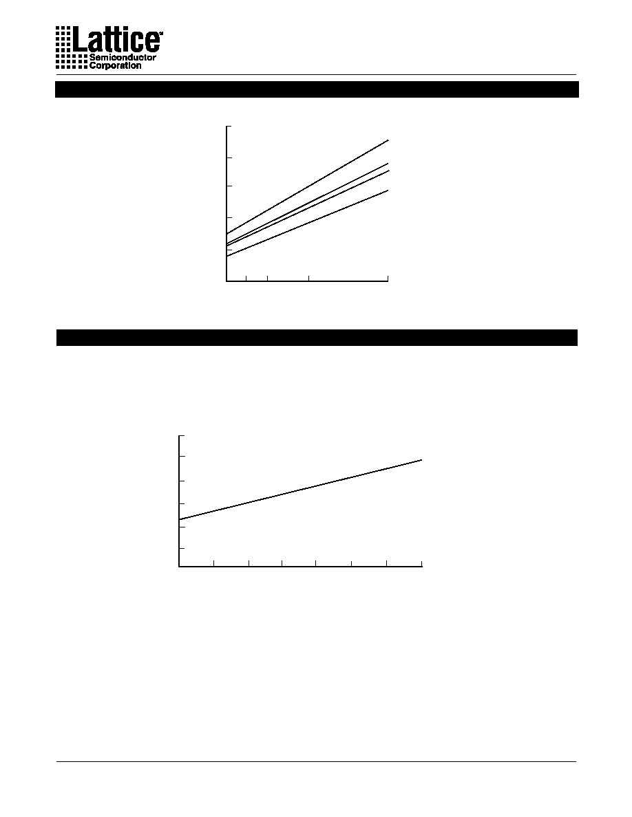
Maximum GRP Delay vs GLB Loads
GLB Load
3.0
5.0
1
8
16
32
GRP Delay (ns)
4.0
4
2.0
6.0
GRP/GLB/1032E
ispLSI and pLSI 1032E-70
ispLSI and pLSI 1032E-90/100
ispLSI and pLSI 1032E-80
ispLSI and pLSI 1032E-125
1.0
Power Consumption
Figure 3. Typical Device Power Consumption vs fmax
Power consumption in the ispLSI and pLSI 1032E device
depends on two primary factors: the speed at which the
device is operating, and the number of product terms
used. Figure 3 shows the relationship between power
and operating speed.
0127/1032E
f
max (MHz)
Notes: Configuration of eight 16-bit counters
Typical current at 5V, 25
∞
C
100
200
300
0
20
40
60
80
100
I
CC (mA)
ispLSI and pLSI 1032E
250
150
350
125
150
CC
I can be estimated for the ispLSI and pLSI 1032E using the following equation:
I (mA) = 15 + (# of PTs * 0.59) + (# of nets * Max freq * 0.0078)
Where:
# of PTs = Number of Product Terms used in design
# of nets = Number of Signals used in device
Max freq = Highest Clock Frequency to the device (in MHz)
The I estimate is based on typical conditions (VCC = 5.0V, room temperature) and an assumption of four GLB
loads on average exists. These values are for estimates only. Since the value of I is sensitive to operating
conditions and the program in the device, the actual I should be verified.
CC
CC
CC
CC
13
Specifications
ispLSI and pLSI 1032E
Pin Description
Input - This pin performs two functions. When
ispEN
is logic low, it functions
as pin to control the operation of the isp state machine. It is a dedicated
input pin when
ispEN
is logic high.
This is a dual function pin. It can be used either as Global Output Enable for
all I/O cells or it can be used as a dedicated input pin.
This is a dual function pin. It can be used either as Global Output Enable for
all I/O cells or it can be used as a dedicated input pin.
Dedicated Clock input. This clock input is brought into the clock distribution
network, and can optionally be routed to any GLB on the device.
Dedicated Clock input. This clock input is connected to one of the clock
inputs of all of the GLBs on the device.
Input/Output Pins - These are the general purpose I/O pins used by the logic
array.
NAME
Table 2-0002A/1032E
PLCC PIN
NUMBERS
DESCRIPTION
26,
30,
34,
38,
45,
49,
53,
57,
68,
72,
76,
80,
3,
7,
11,
15,
27,
31,
35,
39,
46,
50,
54,
58,
69,
73,
77,
81,
4,
8,
12,
16,
28,
32,
36,
40,
47,
51,
55,
59,
70,
74,
78,
82,
5,
9,
13,
17,
I/O 0 - I/O 3
I/O 4 - I/O 7
I/O 8 - I/O 11
I/O 12 - I/O 15
I/O 16 - I/O 19
I/O 20 - I/O 23
I/O 24 - I/O 27
I/O 28 - I/O 31
I/O 32 - I/O 35
I/O 36 - I/O 39
I/O 40 - I/O 43
I/O 44 - I/O 47
I/O 48 - I/O 51
I/O 52 - I/O 55
I/O 56 - I/O 59
I/O 60 - I/O 63
29,
33,
37,
41,
48,
52,
56,
60,
71,
75,
79,
83,
6,
10,
14,
18
66
Y1
20
Y0
42
MODE*/IN 1
Ground (GND)
GND
Vcc
VCC
21, 65
NC
GOE 0/IN 4
Dedicated input pins to the device.
IN 6, IN 7
GOE 1/IN 5
2,
84
67
19
Input - Dedicated in-system programming enable input pin. This pin is
brought low to enable the programming mode. The MODE, SDI, SDO and
SCLK options become active.
23
ispEN**/NC
Input - This pin performs two functions. When
ispEN
is logic low, it functions
as an input pin to load programming data into the device. SDI/IN 0 is also
used as one of the two control pins for the isp state machine. It is a
dedicated input pin when
ispEN
is logic high.
25
SDI*/IN 0
44
SDO*/IN 2
Output/Input - This pin performs two functions. When
ispEN
is logic low, it
functions as an output pin to read serial shift register data. It is a dedicated
input pin when
ispEN
is logic high.
61
SCLK*/IN 3
Input - This pin performs two functions. When
ispEN
is logic low, it functions
as a clock pin for the Serial Shift Register. It is a dedicated input pin when
ispEN
is logic high.
Active Low (0) Reset pin which resets all of the GLB and I/O registers in the
device.
24
RESET
Dedicated Clock input. This clock input is brought into the clock distribution
network, and can optionally be routed to any GLB and/or any I/O cell on the
device.
63
Y2
Dedicated Clock input. This clock input is brought into the clock distribution
network, and can optionally be routed to any I/O cell on the device.
62
Y3
1,
22,
43,
64
12,
1,
26,
51,
76,
64
2, 24, 25, No connect.
27, 49, 50,
52, 74, 75,
77, 99, 100
* ispLSI 1032E only
** ispEN for ispLSI 1032E; NC for pLSI 1032E, must be left floating or tied to V , must not be grounded or tied
to any other signal.
CC
TQFP PIN
NUMBERS
17,
21,
29,
33,
40,
44,
48,
56,
67,
71,
79,
83,
90,
94,
98,
6,
18,
22,
30,
34,
41,
45,
53,
57,
68,
72,
80,
84,
91,
95,
3,
7,
19,
23,
31,
35,
42,
46,
54,
58,
69,
73,
81,
85,
92,
96,
4,
8,
20,
28,
32,
36,
43,
47,
55,
59,
70,
78,
82,
86,
93,
97,
5,
9
65
11
37
89,
87
66
10
14
16
39
60
15
62
61
13, 38,
63,
88
14
Specifications
ispLSI and pLSI 1032E
ispLSI and pLSI 1032E 84-Pin PLCC Pinout Diagram
I/O 38
I/O 37
I/O 36
I/O 35
I/O 34
I/O 33
I/O 32
**GOE 0/IN 4
Y1
VCC
GND
Y2
Y3
*SCLK/IN 3
I/O 31
I/O 30
I/O 29
I/O 28
I/O 27
I/O 26
I/O 25
I/O 57
I/O 58
I/O 59
I/O 60
I/O 61
I/O 62
I/O 63
IN 7
Y0
VCC
GND
*ispEN/NC
RESET
*SDI/IN 0
I/O 0
I/O 1
I/O 2
I/O 3
I/O 4
I/O 5
I/O 6
I/O 56
I/O 55
I/O 54
I/O 53
I/O 52
I/O 51
I/O 50
I/O 49
I/O 48
IN 6
GND
**GOE 1/IN 5
I/O 47
I/O 46
I/O 45
I/O 44
I/O 43
I/O 42
I/O 41
I/O 40
I/O 39
I/O 7
I/O 8
I/O 9
I/O 10
I/O 11
I/O 12
I/O 13
I/O 14
I/O 15
*MODE/IN 1
GND
*SDO/IN 2
I/O 16
I/O 17
I/O 18
I/O 19
I/O 20
I/O 21
I/O 22
I/O 23
I/O 24
12
13
14
15
16
17
18
19
20
21
22
23
24
25
26
27
28
29
30
31
32
74
73
72
71
70
69
68
67
66
65
64
63
62
61
60
59
58
57
56
55
54
ispLSI 1032E
pLSI 1032E
Top View
* Pins have dual function capability for ispLSI 1032E only (except pin 23, which is ispEN only).
0123-32-isp
** Pins have dual function capability which is software selectable.
33 34 35 36 37 38 39 40 41 42 43 44 45 46 47 48 49 50 51 52 53
11 10 9
8
7
6
5
4
3
2
1 84 83 82 81 80 79 78 77 76 75
Pin Configurations
15
Specifications
ispLSI and pLSI 1032E
NC
NC
I/O 57
I/O 58
I/O 59
I/O 60
I/O 61
I/O 62
I/O 63
IN 7
Y0
VCC
GND
ispEN
RESET
*SDI/IN 0
I/O 0
I/O 1
I/O 2
I/O 3
I/O 4
I/O 5
I/O 6
NC
NC
NC
NC
I/O 38
I/O 37
I/O 36
I/O 35
I/O 34
I/O 33
I/O 32
**GOE 0/IN 4
Y1
VCC
GND
Y2
Y3
*SCLK/IN 3
I/O 31
I/O 30
I/O 29
I/O 28
I/O 27
I/O 26
I/O 25
NC
NC
NC
NC
I/O 56
I/O 55
I/O 54
I/O 53
I/O 52
I/O 51
I/O 50
I/O 49
I/O 48
IN 6
GND
**GOE 1/IN 5
I/O 47
I/O 46
I/O 45
I/O 44
I/O 43
I/O 42
I/O 41
I/O 40
I/O 39
NC
NC
NC
NC
I/O 7
I/O 8
I/O 9
I/O 10
I/O 11
I/O 12
I/O 13
I/O 14
I/O 15
*MODE/IN1
GND
*SDO/IN 2
I/O 16
I/O 17
I/O 18
I/O 19
I/O 20
I/O 21
I/O 22
I/O 23
I/O 24
NC
NC
1
2
3
4
5
6
7
8
9
10
11
12
13
14
15
16
17
18
19
20
21
22
23
24
25
75
74
73
72
71
70
69
68
67
66
65
64
63
62
61
60
59
57
56
55
54
53
52
51
26
27
28
29
30
31
32
33
34
35
36
37
38
39
40
41
42
43
44
45
46
47
48
49
50
100
99
98
97
96
95
94
93
92
91
90
89
88
87
86
85
84
83
82
81
80
79
78
77
76
58
ispLSI 1032E
Top View
* Pins have dual function capability.
** Pins have dual function capability which is software selectable.
0766A-32E-isp
ispLSI 1032E 100-Pin TQFP Pinout Diagram
Pin Configurations
16
Specifications
ispLSI and pLSI 1032E
Note:
Use ispLSI f
or all ne
w designs.
Part Number Description
Device Number
Grade
Blank = Commercial
I = Industrial
1032E
XXX
X
X
X
Speed
125 = 125 MHz
f
max
100 = 100 MHz
f
max
90 = 90 MHz
f
max
80 = 80 MHz
f
max
70 = 70 MHz
f
max
Power
L = Low
Package
J = PLCC
T = TQFP
≠
Device Family
0212/1032E
(is)pLSI
ispLSI and pLSI 1032E Ordering Information
100
100
84-Pin PLCC
10
10
ispLSI 1032E-100LJ
100-Pin TQFP
ispLSI 1032E-100LT
pLSI
Table 2-0041A/1032E
90
90
84-Pin PLCC
10
10
ispLSI 1032E-90LJ*
100-Pin TQFP
ispLSI 1032E-90LT*
80
12
84-Pin PLCC
ispLSI 1032E-80LJ*
FAMILY
fmax (MHz)
125
ORDERING NUMBER
PACKAGE
tpd (ns)
7.5
ispLSI
84-Pin PLCC
ispLSI 1032E-125LJ
80
70
70
100-Pin TQFP
84-Pin PLCC
12
15
15
ispLSI 1032E-80LT*
ispLSI 1032E-70LJ
100-Pin TQFP
ispLSI 1032E-70LT
125
100-Pin TQFP
7.5
ispLSI 1032E-125LT
80
70
84-Pin PLCC
12
15
pLSI 1032E-80LJ*
84-Pin PLCC
pLSI 1032E-70LJ
125
100
84-Pin PLCC
7.5
10
pLSI 1032E-125LJ
84-Pin PLCC
pLSI 1032E-100LJ
90
84-Pin PLCC
10
pLSI 1032E-90LJ*
COMMERCIAL
*ispLSI 1032E-100 recommended for new designs.
Table 2-0041B/1032E
FAMILY
fmax (MHz)
70
70
ORDERING NUMBER
PACKAGE
84-Pin PLCC
100-Pin TQFP
tpd (ns)
15
15
ispLSI
ispLSI 1032E-70LJI
ispLSI 1032E-70LTI
INDUSTRIAL
Copyright © 1997 Lattice Semiconductor Corporation.
E2CMOS, GAL, ispGAL, ispLSI, pLSI, pDS, Silicon Forest, UltraMOS, Lattice Semiconductor, L (stylized) Lattice
Semiconductor Corp., L (stylized) and Lattice (design) are registered trademarks of Lattice Semiconductor Corporation.
Generic Array Logic, ISP, ispATE, ispCODE, ispDOWNLOAD, ispDS, ispDS+, ispGDS, ispGDX, ispHDL, ispJTAG, ispStarter,
ispSTREAM, ispTEST, ispTURBO, ispVECTOR, ispVerilog, ispVHDL, Latch-Lock, LHDL, pDS+, RFT, Total ISP and Twin
GLB are trademarks of Lattice Semiconductor Corporation. ISP is a service mark of Lattice Semiconductor Corporation. All
brand names or product names mentioned are trademarks or registered trademarks of their respective holders.
Lattice Semiconductor Corporation (LSC) products are made under one or more of the following U.S. and international
patents: 4,761,768 US, 4,766,569 US, 4,833,646 US, 4,852,044 US, 4,855,954 US, 4,879,688 US, 4,887,239 US, 4,896,296
US, 5,130,574 US, 5,138,198 US, 5,162,679 US, 5,191,243 US, 5,204,556 US, 5,231,315 US, 5,231,316 US, 5,237,218 US,
5,245,226 US, 5,251,169 US, 5,272,666 US, 5,281,906 US, 5,295,095 US, 5,329,179 US, 5,331,590 US, 5,336,951 US,
5,353,246 US, 5,357,156 US, 5,359,573 US, 5,394,033 US, 5,394,037 US, 5,404,055 US, 5,418,390 US, 5,493,205 US,
0194091 EP, 0196771B1 EP, 0267271 EP, 0196771 UK, 0194091 GB, 0196771 WG, P3686070.0-08 WG. LSC does not
represent that products described herein are free from patent infringement or from any third-party right.
The specifications and information herein are subject to change without notice. Lattice Semiconductor Corporation (LSC)
reserves the right to discontinue any product or service without notice and assumes no obligation to correct any errors
contained herein or to advise any user of this document of any correction if such be made. LSC recommends its customers
obtain the latest version of the relevant information to establish, before ordering, that the information being relied upon is
current.
LSC warrants performance of its products to current and applicable specifications in accordance with LSC's standard
warranty. Testing and other quality control procedures are performed to the extent LSC deems necessary. Specific testing of
all parameters of each product is not necessarily performed, unless mandated by government requirements.
LSC assumes no liability for applications assistance, customer's product design, software performance, or infringements of
patents or services arising from the use of the products and services described herein.
LSC products are not authorized for use in life-support applications, devices or systems. Inclusion of LSC products in such
applications is prohibited.
LATTICE SEMICONDUCTOR CORPORATION
5555 Northeast Moore Court
Hillsboro, Oregon 97124 U.S.A.
Tel.: (503) 681-0118
FAX: (503) 681-3037
http://www.latticesemi.com
July 1997